In hindsight, Lynda, Chip Verification Engineer of Tencent, thought joining the company could’ve been a “hasty” decision.
“Where’s our simulation tool?”
“Well, still in progress.”
“What about the verification environment?”
“Nothing yet.”
“Then…what about the verification process?”
“We don’t have that neither.”
The conversation happened in January 2019. After joining Tencent, Lynda felt all pumped up – she rolled up her sleeves and was ready to achieve something big at work, only to find out three “No”s upon her arrival.
“We’re basically making chips from zero.”
During the interview, Henry, who led the chip design project, just wanted to give Lynda a heads up about the current situation.
However, Lynda wanted to participate in the whole process of chip development, so for her, starting from scratch didn’t sound as intimidating. But little did she know that even the most basic necessities, such as the simulation tools, verification environment, and verification process, were, in fact, luxury.
As we all know, chip research and development hold high standards, require intense investment, and bear high risks. Often times, verification engineers are the gatekeepers. Software development usually allows coders to fix bugs in later stages, but with chips, it’s a different story. If problems are left unidentified during the early stages of chip development, once taped out, the chip becomes nothing but a decorative silicon wafer.
Therefore, many chip companies maintain a 1:3 ratio of design engineers to verification engineers. In Penglai Laboratory, however, there were only Lynda, another verification engineer, and some verification conditions without a single line of code.
Only then did Lynda begin to understand what Henry meant by “starting from zero” and what an uphill battle she faced.
1
A Team Near Disbandment
According to Xie Ming, Vice President of Tencent Cloud and General Manager of the Cloud Architecture Platform Department, in this competition of chips, Tencent “felt imperative and has been planning for a long time”.
This team was responsible for the backend architecture of the national-level software applications such as QQ, standing on the front line of Tencent’s massive business, and thus understood deeply the magnified value of the foundational technological innovation to the upper-level applications.
In 2013, QQ Album developed into Tencent’s largest storage business.
It became an urgent need to provide users with faster access to their photos and with smoother user experience. All this, translating into technological terms, were questions like could we transcode images faster? Could we compress photos without compromising image quality? Could we store them at a lower cost?
Technicians asked themselves repeatedly.
With endless updates in software architecture, the team realized that only by making innovative progress in hardware could they achieve revolutionary breakthroughs.

How does a software team go hardware?
After some research, they decided to test the waters with FPGA (a field-programmable gate array). Compared with chips, FPGAs have higher fault tolerance, but are balanced in terms of throughput, delay, power consumption, and flexibility. Especially when processing massive data, FPGA shows a significant advantage of ultra-low latency compared to GPU.
Facts also solidified these statements. In 2015, the image encoding FPGA that the team researched and developed achieved higher compression rate and lower latency than CPU encoding and software encoding methods, and greatly reduced QQ Album’s storage costs. The team saw the possibility of further exploring in the FPGA direction.
Around 2016, the AI mania ignited by AlphaGo brought FPGA into the mainstream. After the team accelerated the CNN algorithm of the deep learning model through FPGA, the processing performance quadrupled comparing to that of a general-purpose CPU, and the unit cost was only 1/3 of the latter.
Although the FPGA was efficient, the technical standards were still relatively high. “If we put FPGAs on cloud, is it a solution that expands its application?”
With such expectations, on January 20th, 2017, Tencent Cloud launched the first-ever FPGA cloud server in China, hoping to empower more enterprises with FPGA by cloud computing.
From the efficiency perspective, companies that perform FPGA hardware programming on FPGA cloud servers could indeed increase the performance to more than 30 times faster than on general-purpose CPU servers, while only paying about 40 percent of the cost of using the CPU. Taking a well-known genetic testing company for example. While the same amount of gene sequences testing requires a week for traditional CPUs to process, FPGAs completed it in a few hours.
However, the cruel reality poured cold water on the team from head to toe, as the cloud-based FPGA failed to quickly prevail the entire industry as expected.
On the one hand, many companies were still unable to independently develop FPGAs and need more supporting services; on the other hand, the rapid decline in GPU costs also caused a huge impact on FPGAs.
The frustration of cloud commercialization dragged the team’s enthusiasm from the peak to the bottom, and also threw a question to the eyes of the entire team: How much value does FPGA have in business? Can FPGAs continue to commercialize?
Due to the impact, the team almost fell apart in 2018, and employees began to leave in groups.
2
Silver Lining: The Born of “Penglai”
Fast-forward to 2019, it was the year of the beginning of large-scale application of artificial intelligence (AI), and both internal and external businesses raised strong demands for AI chips.
After the setback of FPGA cloud servers, Tencent needed to rethink the strategy for hardware.
AI chips, or not?
When this question was brought to the table, there were doubts and disapproval from the management, worrying that tech staff were simply too heated over the trend, chasing the clout, or just being conceited. However, no actions were taken to explicitly prohibit small teams from exploring on the subject.
Gradually, it became a consensus of everyone to test the waters in small-scale, low-cost, and application-specific scenarios.
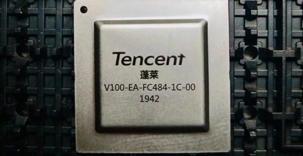
The Cloud Architecture Platform Department finalized the AI reasoning direction for the first chip and named it “Penglai(蓬莱)”, in hopes that it could stand firmly despite of the turbulent waves, just like the fairy mountains in ancient Chinese mythology.
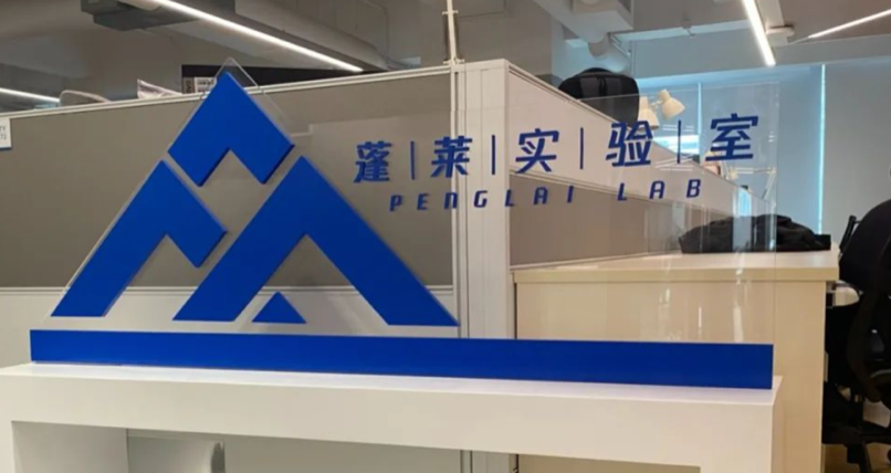
This hardware squad was also officially named “Penglai Laboratory”.
After FPGA, Penglai Lab was quite proficient in hardware programming languages and accumulated many platform-based designs in terms of standard interfaces and buses. However, the requirements between research and development were very different.
If making FPGA was like to play with building blocks, then making chips was to create building blocks from timbers. An FPGA’s bug could always be reprogrammed later but a chip had only one chance for tape-out. Once it went South, all the hard work would be in vain.
In addition, the sources of FPGA were preset and ready-made, but for chips, the sources were undefined and required customization.
In one word, it was all about “optimization”: to achieve the biggest goal with the least resources.
Chip architecture engineer, Rick, used “renovation” to “reconstruction” to describe the entire Penglai project.
At first, the team thought it would be easy to borrow from the previous FPGA technology and apply it to the current chip development. However, assumptions were always simpler than actions after all. During the exploration stage, the team soon discovered only limited numbers of FPGA architectures could be of direct reuse in chip programming. Hence, they needed to reorganize the original architecture, and the number of codes rewritten reached as high as 85 percent.
For the most essential part like DDR memory storage, chip manufacturers usually appoint verification experts in charge. However, Penglai Laboratory, which was just starting up, could not benefit from such advantage. The best it could do was catching up.
In January 2020, the Penglai chips were taped out and delivered to Shenzhen. It was about the same time the pandemic hit across the nation, and people started to work from home.
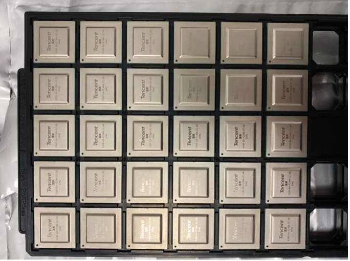
The taped-out Penglai chips arrived at Shenzhen
Henry took the package with gloves on. He carefully disinfected it with medical alcohol and carried it to the empty office building. With the windows open and fans on, several colleagues and he started the “lighting” process.
The so-called “lighting process” was to power up the chip with electricity. It was to, first, check if there was a short circuit or smoke, and then test some basic functions.
Whether it was a real chip or just a non-functional silicon wafer, they would soon find out.
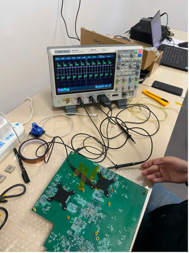
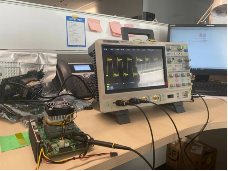
The clock that tested Penglai chips
As a result, the chip still exhibited no sight of the clock frequency. One must know that the clock frequency was like the “metronome” of the chip. Without it, the different modules of the chip could not work together, just like an unsynchronized watch.
Is there a problem with this chip? The research staff switched to another chip but still, no signal output observed.
After the third piece, still nothing.
Dead silence in the room. No staff dared to make another move.
Some researchers could not help but starting to joke around – “is it time to go home and polish our CVs again?” But what’s lingering on their minds were nothing but doubts:
Despite limited staff, scarce resources, and lack of experience, the researchers from Penglai Lab started from scratch. And this time, from chip designers to verification engineers, people were all quite confident about every step they took. What could possibly go wrong then?
With an extremely heavy heart, the staff prepared the board, powered on, and looked for the signal once again…
The fourth chip was “lit up”! And so were the rest of the chips.
It turned out that normally, the defective rate of chips made with the 28-nanometer technology was only 3 percent. In this random test, the first three chips happened to fall out of the margin of error, causing intensive stress to the researchers in the room.
After these twists and turns, Tencent’s first chip was finally born.
3
The Next Level: To The “Zixiao” Cloud
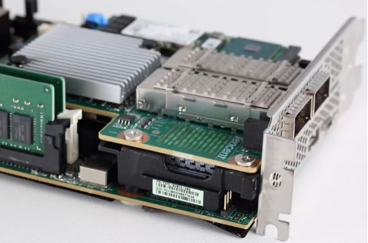
Penglai chip’s performance in real-life application lived up to expectations, helping Tencent launch China’s first smart microscope approved for clinical use in hospitals. The smart microscope could automatically identify medical images, calculate the number of cells, and display them directly on the field of view. And the Penglai chips they carry also function perfectly as designed.
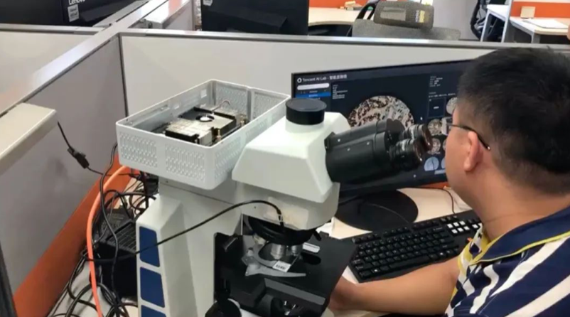
Penglai chips being tested on smart microscopes
Efficiently creating chips that stand the test of direct applications and exhibit excellent performance is a road for Tencent.
The advent of the terminal Penglai chip only completed the task from 0 to 1. The team were already excited to go from 1 to N and marched towards the large-scale cloud chips.
Alex, Head of Penglai Lab, dubbed the large-scale chip project application as “Series A Financing”.
After the initial experiment, the team must explain to the management why they needed to invest more in large-scale chips? Could they lead the competition in the short and long run? And how to link the project with the internal and external business to create more values?
This time, however, the decisions were much easier to make for Tencent.
Penglai’s proven success bolstered the team’s confidence. As Penglai Lab grew bigger, it also accomplished many transformations, gradually building up a rigorious, integrated, and standardized process for chip research and development.
This was already a “regular army”.
More importantly, the team solidified Tencent’s advantage and position as a chip maker.
Xie Ming explained that from an industry point of view, apart from technology and craftsmanship, the biggest difficulty was the “definition” of chips. The advantage of traditional chip manufacturers obviously lied in the former. If we started to align with user’s demand only after the chip was made, the real functions of the chips might get wasted in many scenarios. The advantage of technology companies, such as Google and Tencent, was that they were on the demand’s side themselves, and thus they had the deepest and most thorough understanding and insight about demand.
With clear directions, qualified technology, and skilled personnel, the team received full support from Lu Shan, Senior Executive Vice President of Tencent and President of TEG (Technical Engineering Division), who provided Penglai Lab with more headcounts and funds with the permission from the General Office.
With the strategic support from the company, the team marched towards bigger challenges with high spirits. Austin, Deputy Director of Penglai Laboratory, decided to divide the “army” into two directions and advance in parallel on “AI inference” and “video encoding & decoding”.
The AI team continued to work on Penglai’s 2.0 version of “Zixiao(紫霄)”. This was the name of the palace where the Hongjun Laozu lived in “Investiture of the Gods”. Building a Zixiao (literally translated as “Purple Sky”) on a stable fairy mountain represented a new ambition:
This time, they aim to be No.1 in the industry.
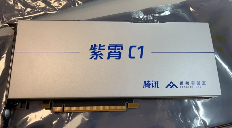
All of Zixiao’s architectures revolved around effective computing power. The team optimized the on-chip cache design and abandoned the GDDR6 memory commonly used by competing products. It adopted advanced 2.5D packaging technology to encapsulate the HBM2e memory and the AI chip together, thereby increasing the memory bandwidth by nearly 40%.
Technological upgrades were advancing by leaps and bounds. Shortly after the establishment of the Zixiao project, the highest performance record in the industry was quickly refreshed by competing products. Although Zixiao’s designed performance remained a considerably “safe” distance from this record, the team decided to continue enhancing.
After research, the team found the competitors added a computer vision CV accelerator and a video codec accelerator inside the chip, which innovatively and greatly reduced the interaction and delay between the AI chip and the x86 CPU.
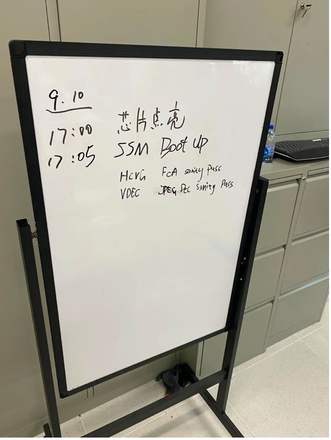
Even with two complex self-developed modules added to the task, the crew still managed to complete the mission as planned, wrapping up the entire process from architecture determination, to verification, and then to the tape-out within 6 months.
On September 10, 2021, Zixiao was successfully “lit up”.
In application scenarios, such as image and video processing, natural language processing, and search recommendation, Zixiao broke the bottleneck that restricted the performance of computing power, and its performance in real-life business applications exceeded the industry standard by two times.
4
Independent Research and The Advent of “Canghai”
On March 5, 2022, Derick and his video encoding & decoding team received the chip “Canghai” back from the tape-out process. The timing coincided with another wave of the pandemic in Shenzhen.
They applied for special entry and returned to the empty office building, and this scene was so similar to when Penglai was “lit up” two years ago.
Unexpectedly, the same twists and turns happened again. After some accidents during the testing process, Tencent’s third chip “Canghai”, which was also the first chip Tencent independently developed, was successfully “lit up”.
From Penglai, to Zixiao, and then to Canghai, from the 28-nanometer technology to the 12-nanometer technology, from 8 staff to more than 100 employees, from the lack of simulation tools to the official completion of the “Tianjian Verification Platform”, from trying to catch up with the industry partners to completing the SoC independently…
Penglai Laboratory accomplished a heartfelt evolution of chip development.
In addition, different from Penglai and Zixiao’s application focus on AI, Canghai was a video transcoding chip.
If the transcoding problem of QQ Album pictures was the earliest opportunity for Penglai Laboratory to make hardware, then the advent of Canghai was a response to the original intention.
Multimedia services evolved from the era of pictures to the era of live audio and video, and 4K/8K ultra-high-definition digital content continued to impact cloud computing infrastructure like a tide. Each additional bit of data would correspondingly increase transcoding computing power and CDN bandwidth costs. This was an intuitive and serious math problem.
The goal of the Canghai team was very clear, that was, to make the industry’s strongest video transcoding chip that maximizes the compression rate.
Fortunately, Tencent’s rich multimedia application scenarios, as well as many live interactive top customers from Tencent Cloud, provided unique analyses and abundant verification conditions for Canghai’s research and development.
The team first launched Canghai’s core self-developed module – the hardware video encoder “Yaochi(瑶池)” – and decided to bring Yaochi to a big test before Canghai completed the R&D progress.
This big test was the MSU World Codecs Comparison 2020. Hosted by Moscow State University (MSU), this competition was one of the most influential contests in the global video compression field, attracting many worldly-renowned technology companies including Intel, Nvidia, Google, Huawei, Alibaba and Tencent to participate.
As a result, Yaochi achieved 1080P@60Hz real-time video encoding and won the first place in various objective metrics such as SSIM (structural similarity), PSNR (peak signal-to-noise ratio) and VMAF (video multi-method assessment fusion). Besides, Yaochi also won the first place in the subjective MSU Human Perceptual Quality Metric by absolute advantage to the second place.
This tough test undoubtedly endorsed Canghai a solid background of technical review.
Turning the ocean into a drop was Canghai’s goal. And finally, it managed to present videos of the same quality with fewer data and smaller bandwidth, with the compression rate being 30+ percent higher than the previous record in the industry.
5
In the “100G” Era, Smart NIC Is Dominating
While multimedia and AI processing were actively seeking changes, the basic cloud servers were also facing similar problems:
When the improvement in performance from software optimization could no longer differ our product from competitor’s, how to accelerate the performance and break the ceiling?
Another department of Tencent had set its sights on the hardware acceleration and the collaboration between software and hardware.
In 2019, Tencent celebrated its milestone in the cloud computing business – the scale of cloud servers exceeded 1 million.
Zou Xianneng, Vice President of Tencent Cloud and General Manager of Tencent’s Network Platform Department, keenly observed that as the number of servers accessing bandwidth continued to increase, the CPU resources used for server network processing also increased.
Could we decrease the costs of server network processing while still providing higher network performance?
Faced with such a challenge of “wanting both X and Y”, Zou Xianneng decided to make a slim transformation for the server: “Unload the burden of network data processing from the CPU.”
Hence, the idea of a “Smart Network Interface Card (Smart NIC)” was born.
Tencent’s Smart NIC “Yinshan”
The so-called Smart NIC, on the one hand, shouldered the external network access of the server like a common network interface card and realized the network interconnection between different servers and data centers. On the other hand, it had additional intelligent units such as CPU/FPGA/memory, which could share part of the server’s virtualized computing tasks, and thus accelerate the overall network and storage performance of the server.
In other words, what the network platform department needed to do was install a new server in the network interface card.
At first, the team wanted to find an off-the-shelf commercial card to reduce the workload.
Hayden, Head of the Network Interface Card Hardware, led the demonstration and research of the project. But the fact that the acceleration engine of commercial chips failing to support private protocols became the first challenge and the biggest obstacle at that time. Several well-known equipment vendors of network interface card also shook their heads after hearing Tencent’s request:
“The function of the current network interface card is pretty simple. Your request is too complicated and hard to achieve.”
There were also sharp questions, too: “There are so many network interface cards with incredibly high requirements on reliability… Can you handle it yourself?”
Should we abort the smart NIC project now, during such early stage?
Zou Xianneng pointed out the direction for the team: “Since smart NIC is a key component of cloud data centers’ pursuit in high performance and optimized cost, if there is no product on the market that meets Tencent’s needs, then we will build one ourselves.”
With a clear direction in mind, the action plan quickly emerged: start with self-developed smart NIC based on FPGA, and then carry out the R&D plan of smart NIC chips.
In September 2020, Tencent’s launched its first-generation, self-developed smart NIC based on FPGA, and named it “Shuishan(水杉)”, in hopes that the product could be as adaptable and fast-growing as the rare tree, Metasequoia.
During the pandemic, while encountering various unexpected demands, the newly born Shuishan were adapting well to the challenges.
Hayden recalled a case where a major client used the UDP audio and video protocol, which was “unreliable” in terms of properties, allowed packet loss, and greatly relied on network throughput and stability, but still required high concurrency and high-quality audio and video transmission effects.
The Shuishan smart NIC rose to the challenge. By greatly improving the network performance of the server, it helped the client complete the 24-hour extreme stress test with zero packet loss, went online stably, and solved the case beautifully.
After the application of Shuishan, the team initiated the R&D progress of the second-generation smart NIC, “Yinshan(银杉)”, in full swing, with an official launch date in October 2021. The network ports of this generation’s smart NIC doubled to 2*100G.
With the support of Yinshan, Tencent Cloud launched the industry’s first self-developed, sixth-generation 100G cloud server.
Its computing performance was improved by up to 220 percent, and its storage performance was improved by up to 100 percent. Compared with the previous generation, the single-node access network bandwidth was up to 4 times higher with the latency reduced by 50 percent.
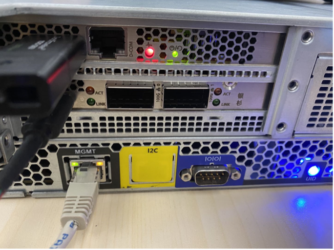
“Yinshan” on the self-developed 100G cloud server
The team was overwhelmingly excited about the huge progress the two smart NICs achieved in offloading network hardware.
While the FPGA strategy gradually approached the bottleneck of performance and power consumption, the network platform department decided to take the initiative again.
6
“Xuanling” Flashes: To Be Continued
Just like that, Tencent’s fourth chip and the first smart NIC chip project came alive.
It also has a “fairy” name – “Xuanling(玄灵)”. According to the schedule, this chip made with the 7-nanometer technology will be taped out by the end of 2022.
Upon command, Hayden quickly set up the Xuanling chip R&D team and began the journey of challenging many “missions impossible”.
From the perspective of performance indicators, the number of devices supported by Xuanling will increase to more than 10K, which is 6 times higher than that of commercial chips. Meanwhile, its performance can be improved by 4 times compared to commercial chips. By offloading functions including virtualization and network/storage IO originally running on the host CPU, the chip can achieve zero occupancy of the host CPU.
This mini and powerful chip fully interprets the “Xuan (mystery)” for the ultimate performance in the future, and the “Ling (spirit)” for the flexible acceleration when facing various business needs.
As of right now, the Xuanling project is under the verification and testing stages of the smart NICs prior to the tape-out process; and on its way to building the next generation’s high-performance network infrastructure of Tencent Cloud;
Penglai Lab’s AI inference chip, Zixiao, and video transcoding chip, Canghai, will soon proceed to the mass production phase and deeply integrate with Tencent’s business;
There are also other new chip projects growing at the moment, continuing to explore technical directions to enrich previous experiences.
The new challenges faced by Tencent’s massive business, as well as the inevitable requirements chased by the rapid development of cloud computing, “forced” Tencent to reflect and embark on this road of chip development. These chips derived from and designed for actual business needs will definitely prove their value as they frequently dive into practical applications in the future.
“The decision to make chips was not a baseless one, nor a hasty one. We knew it from the beginning that Tencent’s demand was large enough for us to do this,” Lu Shan said.
Since 2010, Tencent has begun to open up its digital technology and connectivity capabilities through cloud services, marching towards this era of digital transformation and this trend of industrial upgrade. Upon entering the wave, Tencent observes that the deep integration of digital and reality is leading the technological trend of the full-real interconnection.
Tencent’s chip business will eventually receive its echo from the ocean of stars where digital and reality truly integrate.